The Great AI Silicon Shortage
Institution: MIT
1 study materials · 3 sections
This course explores the critical supply chain constraints currently throttling the global AI industry as it transitions to advanced manufacturing nodes. It examines the specific bottlenecks within TSMC's N3 process, the scarcity of High Bandwidth Memory (HBM), and the physical limitations of datacenter infrastructure. Students will analyze how hyperscalers are navigating these shortages and the resulting shift in global foundry strategies and capital expenditure trends.
Course Sections
The TSMC N3 Fabrication Crisis
Key concepts: TSMC N3 Process Node · Wafer Shortages · AI Accelerator Demand
An analysis of the transition to the N3 process node and why fabrication capacity is failing to meet AI accelerator demand.
The TSMC N3 Fabrication Crisis
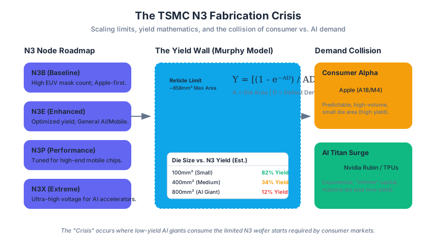
The semiconductor industry is currently navigating a period of unprecedented structural tension, colloquially termed "The Great AI Silicon Shortage." At the epicenter of this crisis is the transition to the TSMC N3 (3-nanometer) process node. While previous node transitions (from N7 to N5) were characterized by predictable mobile-led adoption, the N3 era is defined by a violent collision between traditional consumer electronics and an insatiable, exponential demand for Artificial Intelligence (AI) accelerators.
This section explores the technical architecture of the N3 node, the mathematical realities of wafer yield at the reticle limit, and the supply chain dynamics that have turned silicon wafers into the world's most contested sovereign resource.
AI_SVGI_SVG## The N3 Process Node: Technical Foundations and Scaling Limits
The TSMC N3 family represents the pinnacle of FinFET (Fin Field-Effect Transistor) scaling. Unlike its primary competitor, Samsung, which transitioned to GAAFET (Gate-All-Around) for its 3nm offerings, TSMC elected to refine the existing FinFET architecture to its absolute physical limit. This decision was driven by the need for manufacturing stability, though it introduced extreme complexities in lithography.
The Physics of N3 Scaling
The transition from N5 to N3 is not a simple photographic reduction. It involves the aggressive use of EUV (Extreme Ultraviolet) Lithography, specifically pushing the numerical aperture (NA) limits of current scanners. In N3, the logic density increases by approximately 1.6x to 1.7x compared to N5.
Definition: Logic Density ($\rho$) Logic density is typically measured in millions of transistors per square millimeter ($MTr/mm^2$). For the N3B (initial) node, the theoretical density targets $\approx 215 MTr/mm^2$, representing a significant leap over N5’s $\approx 138 MTr/mm^2$.
N3 Node Variants
TSMC does not offer a single "N3" process but rather a roadmap of iterative refinements designed to balance yield, power, and performance.
| Node Variant | Target Market | Key Characteristic | Status |
|---|---|---|---|
| N3B | Early Adopters (Apple) | Original 3nm, high EUV mask count, complex | Production |
| N3E | General AI/Mobile | "Enhanced" - better yields, slightly lower density than N3B | Volume Production |
| N3P | Performance Mobile | Performance boost via process tuning | Risk Production |
| N3X | HPC / AI Accelerators | Ultra-high voltage support for maximum clock speeds | Development |
The "Crisis" stems from the fact that while N3E is the "sweet spot" for yield, the requirements for AI accelerators (like Nvidia's Rubin or Google’s TPU v6) demand the performance characteristics of N3P or N3X, which are the most difficult to manufacture at scale.
The Mathematics of the Wafer Shortage: Yield and Reticle Limits
To understand why N3 wafers are in such short supply, we must examine the relationship between chip area, defect density, and the Reticle Limit.
The Reticle Limit Constraint
Most high-end AI accelerators are "reticle-sized" chips. The reticle limit is the maximum physical area a photolithography tool can expose in a single step, currently fixed at approximately $26mm \times 33mm = 858mm^2$.
As AI models grow, designers push chips to this $858mm^2$ limit to maximize on-chip memory and compute units. However, as the area ($A$) of a die increases, the probability of a fatal defect ($D$) ruining the chip increases exponentially.
The Murphy Yield Model
We can model the expected yield ($Y$) of N3 wafers using the Murphy Model, which is more realistic for advanced nodes than the simpler Poisson distribution:
$$Y = \left( \frac{1 - e^{-AD}}{AD} \right)^2$$
Where:
- $A$ = Area of the die ($mm^2$)
- $D$ = Defect density (defects per $mm^2$)
Worked Example: N5 vs. N3 Yield Comparison Assume a defect density $D = 0.05$ for a mature N5 process and $D = 0.1$ for an early-stage N3 process. Let's calculate the yield for a large AI accelerator ($A = 800mm^2$).
-
N5 Yield: $$Y_{N5} = \left( \frac{1 - e^{-(800 \cdot 0.05)}}{800 \cdot 0.05} \right)^2 = \left( \frac{1 - e^{-40}}{40} \right)^2 \approx 0.000625 \text{ (effectively 0.06%)}$$ Note: This illustrates why massive chips are often "binning-dependent" or use multi-die chiplet designs.
-
N3 Yield (Early Stage): If the defect density is higher ($0.1$), the yield for a monolithic $800mm^2$ die becomes mathematically negligible. This forces a transition to Chiplets, where smaller dies (e.g., $200mm^2$) are manufactured and then interconnected.
| Die Area ($mm^2$) | N3 Yield (Est. $D=0.07$) | Good Dies per Wafer (300mm) |
|---|---|---|
| 100 (Small) | 82% | ~580 |
| 400 (Medium) | 34% | ~60 |
| 800 (Reticle Limit) | 12% | ~8 |
The "Crisis" is exacerbated here: because AI chips are huge, they consume more wafer area per functional unit, and their low yields mean more wafers must be started to reach a target volume of working chips.
AI Accelerator Demand: The Rubin and TPU Surge
The primary drivers of the N3 shortage are the next-generation AI architectures. Historically, Apple was the sole "Alpha" customer for new TSMC nodes. However, the generative AI boom has introduced two new titans: Nvidia and Hyperscalers (Google, Amazon, Meta).
Nvidia Rubin Architecture
Nvidia’s transition from the Hopper (N4) and Blackwell (N4P) architectures to the Rubin architecture marks a shift to the N3 node. Unlike Blackwell, which utilized a "reticle-busting" dual-die approach on 4nm, Rubin is designed to leverage the density of N3 to pack more CUDA cores and HBM3e/4 controllers into the same footprint.
Hyperscaler Silicon (TPU/Trainium)
Google’s TPU v6 and Amazon’s Trainium 3 are moving to N3 to achieve the energy efficiency required for massive-scale inference. Because these companies have "infinite" Capex (Capital Expenditure), they are willing to outbid traditional smartphone manufacturers for wafer starts.
Key Insight: The Capex War In 2024-2025, the "Big Four" (Microsoft, Google, Meta, AWS) have projected a combined Capex exceeding $200 billion. A significant portion of this is earmarked for AI hardware. This financial firehose has disrupted the traditional "Smartphone First" allocation logic at TSMC.
The HBM and CoWoS Bottleneck
It is a common misconception that the N3 crisis is solely about the logic wafer. In reality, the crisis is a multi-dimensional constraint involving High Bandwidth Memory (HBM) and CoWoS (Chip-on-Wafer-on-Substrate) packaging.
CoWoS: The Invisible Ceiling
CoWoS is a 2.5D packaging technology where the logic die and HBM stacks are placed on a silicon interposer. Even if TSMC produces an N3 wafer perfectly, the chip cannot be used until it is packaged.
- Interposer Shortage: The interposers themselves are large pieces of silicon, often 2x or 3x the size of the logic die. They compete for capacity on older, "legacy" nodes (like 65nm).
- HBM3e/4 Integration: HBM requires vertical stacking using Through-Silicon Vias (TSVs). The alignment precision required for N3-class chips is so high that assembly yields are currently a major bottleneck.
| Constraint | Impact on Supply | Mitigation Strategy |
|---|---|---|
| N3 Wafer Starts | Limits raw chip volume | Expansion of Fab 18 in Tainan |
| CoWoS Capacity | Limits final assembly | Outsourcing to Amkor/Intel Foundry |
| HBM Supply | Limits memory-bound AI tasks | Diversification (SK Hynix, Samsung, Micron) |
Supply Chain Wars: Winners and Losers
The N3 crisis has created a "bifurcated" semiconductor market.
The Winners: The "First Class" Customers
- Apple: Maintains a "Golden Contract" with TSMC, often securing 100% of initial N3 capacity for the iPhone's A-series and Mac's M-series chips.
- Nvidia: Due to its massive margins (70-80%), Nvidia can afford the $20,000+ price tag of an N3 wafer.
- TSMC: As the sole provider of reliable 3nm FinFET, TSMC possesses absolute pricing power.
The Losers: The "Displaced"
- Mid-tier Smartphone Vendors: Companies like Xiaomi or Oppo are forced to stay on N4 or N5 nodes longer than planned, as they cannot compete with AI margins.
- Automotive: While automotive doesn't use 3nm for power electronics, the competition for cleanroom space and EUV tools at TSMC indirectly delays the expansion of the older nodes they rely on.
Strategic Diversification and Foundry Shifts
To mitigate the N3 crisis, the industry is seeing a desperate push for Foundry Diversification.
- Intel Foundry Services (IFS): Intel’s 18A node is positioned as a direct competitor to TSMC N3P. Microsoft has already signed on as a lead customer to hedge against TSMC shortages.
- Samsung Foundry: Despite yield struggles with its 3nm GAA process, Samsung is attracting customers like Groq and potentially Meta, who are looking for "second-source" insurance.
- Edge AI Re-allocation: There is a growing trend of "Small Language Models" (SLMs) designed to run on N4 or N5 silicon, intentionally avoiding the N3 supply crunch by optimizing software for older hardware.
Common Pitfalls and Misconceptions
- "3nm means 3 nanometers": In modern semiconductor manufacturing, the "3nm" name is a marketing term. No physical feature (gate length or pitch) is actually 3nm. The naming refers to the equivalent performance jump relative to the previous generation's scaling.
- "Just build more Fabs": A modern N3-capable fab costs roughly $20 billion and takes 3-5 years to reach volume production. The crisis cannot be "built out of" in a single fiscal year.
- "Yield is the only cost": At N3, the cost of design (EDA tools, IP licensing, validation) exceeds $500 million for a complex chip. Many companies are "priced out" of N3 not by wafer costs, but by the R&D required to use the node.
AI_STUDY_GUIDEI_STUDY_GUIDE### Key Terms to Remember
- FinFET: The 3D transistor structure used in N3.
- EUV Multi-patterning: The process of using multiple EUV exposures to define features smaller than the tool's native resolution.
- WSPM: Wafer Starts Per Month—the standard metric for fab capacity.
- Interposer: The silicon bridge in CoWoS packaging that connects the GPU to its memory.
Critical Thinking Questions
- How does the Murphy Yield Model explain the industry's aggressive shift toward chiplet-based architectures for AI?
- Why did TSMC's decision to stay with FinFET for N3 (while Samsung moved to GAA) prove to be a strategic advantage during the AI boom?
- If Hyperscaler Capex continues to grow at 20% CAGR, what happens to the pricing of consumer electronics that rely on the same leading-edge nodes?
AI_FLASHCARDSI_FLASHCARDS N3B: TSMC's first 3nm node; high density but high cost/complexity.
- N3E: The "workhorse" 3nm node; improved yields, used by most AI companies.
- Reticle Limit: ~858mm²; the physical "ceiling" for chip size.
- CoWoS: Chip-on-Wafer-on-Substrate; the packaging bottleneck for AI chips.
- HBM3e: High Bandwidth Memory; the specialized RAM required for AI accelerators.
- EUV: Extreme Ultraviolet Lithography; the light source required for sub-7nm features.
- Wafer Price: The cost of an N3 wafer is estimated at >$20,000, vs ~$15,000 for N5.
- PPA: Power, Performance, and Area; the three metrics used to evaluate node transitions.
Memory Constraints and Datacenter Bottlenecks
Key concepts: HBM (High Bandwidth Memory) · Cleanroom Space · Datacenter Bottlenecks
Exploring the secondary bottlenecks in AI production: HBM supply and the physical limits of cleanroom space.
Memory Constraints and Datacenter Bottlenecks
The global semiconductor landscape is currently defined by a singular, frantic pursuit: the acquisition of compute density. While much of the public discourse focuses on the raw transistor counts of logic chips like Nvidia’s Blackwell or Google’s TPU v6, the actual "Great AI Silicon Shortage" is a multi-front war fought across the dimensions of memory bandwidth, advanced packaging, and the physical constraints of the datacenter floor.
As the industry transitions to the TSMC N3 (3nm) process node, the bottleneck has shifted. It is no longer just about who can design the best architecture, but who can secure the physical resources—High Bandwidth Memory (HBM), cleanroom floor space, and power-dense datacenter racks—to actually deploy that architecture at scale. This article explores the technical and logistical constraints that define the current era of AI infrastructure.
AI_SVGI_SVG--
High Bandwidth Memory (HBM): The Memory Wall
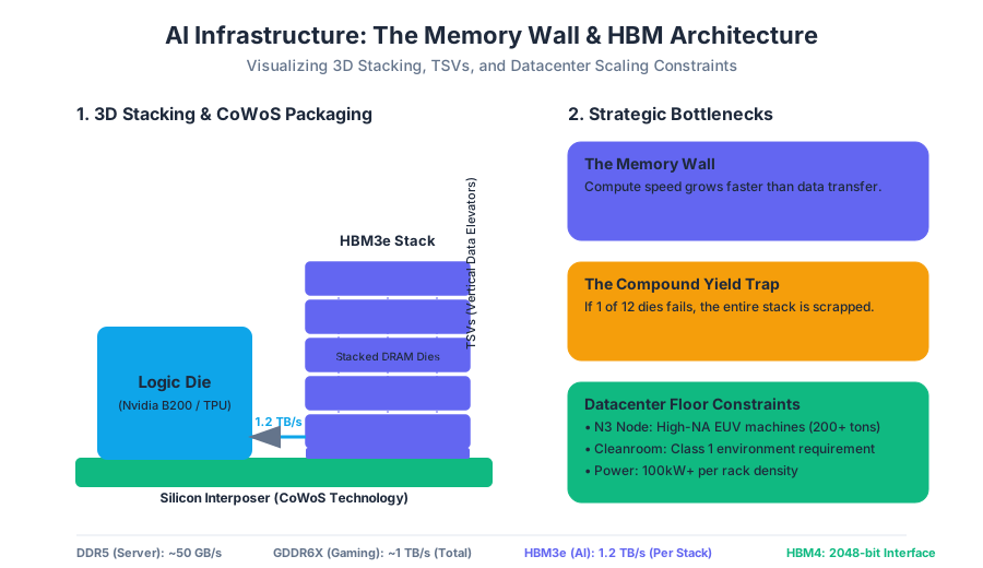
In the context of Large Language Models (LLMs), the "Memory Wall" refers to the growing disparity between the speed of processors and the speed at which data can be moved from memory to those processors. High Bandwidth Memory (HBM) was engineered specifically to bridge this gap.
1. What it is
Definition: HBM is a specialized computer memory interface for 3D-stacked synchronous dynamic random-access memory (SDRAM). It utilizes Through-Silicon Vias (TSVs) and microbumps to connect multiple DRAM dies vertically, significantly reducing the physical distance data must travel and increasing the number of available data pins.
Mathematically, the bandwidth $B$ of a memory system is defined as: $$B = f \times w \times n$$ Where:
- $f$ is the clock frequency.
- $w$ is the bus width (bits per channel).
- $n$ is the number of channels.
While standard GDDR6 memory relies on high frequencies ($f$) to achieve speed, HBM focuses on a massive increase in bus width ($w$) and channel count ($n$) by stacking dies.
2. Why it matters
AI workloads are inherently "memory-bound." Training a model with trillions of parameters requires constant shuffling of weights and gradients between the processor and memory. If the memory bandwidth is insufficient, the expensive AI accelerator (costing $30,000+) sits idle, waiting for data—a state known as "starvation."
3. How it works: The 3D Stacking Architecture
HBM achieves its performance through a radical departure from traditional PCB-based memory placement:
- Vertical Stacking: 8, 12, or even 16 DRAM dies are stacked on top of a logic base die.
- TSVs: Thousands of microscopic holes are etched through the silicon dies, filled with copper, and used as vertical "elevators" for electrical signals.
- Microbumps: These act as the solder points between the layers. The density of these bumps is orders of magnitude higher than traditional flip-chip packaging.
- The Interposer: The HBM stack and the GPU/TPU are placed on a silicon interposer (a large, flat piece of silicon with dense routing). This is the core of TSMC’s CoWoS (Chip on Wafer on Substrate) technology.
4. Comparison of Memory Technologies
The following table illustrates why HBM has become the non-negotiable standard for AI accelerators.
| Feature | DDR5 (Server) | GDDR6X (Gaming) | HBM3e (AI/HPC) |
|---|---|---|---|
| Architecture | DIMM Modules | Discrete Chips | 3D Stacked |
| Bus Width | 64-bit | 32-bit per chip | 1024-bit per stack |
| Bandwidth | ~50 GB/s | ~1 TB/s (system total) | ~1.2 TB/s (per stack) |
| Power Efficiency | Moderate | Low (High $f$ = High Heat) | High (pJ/bit) |
| Physical Footprint | Large | Medium | Minimal (Integrated) |
5. Variations and Extensions: HBM3e to HBM4
The industry is currently transitioning from HBM3e (found in Nvidia H200/B200) to HBM4.
- HBM4 will move to a 2048-bit interface, doubling the bus width again.
- It will also likely involve "Direct Bonding" (copper-to-copper), removing the need for microbumps and further reducing the stack height and thermal resistance.
6. Common Pitfalls: The Yield Trap
The primary pitfall of HBM is the Compound Yield Loss. If you stack 12 DRAM dies and one die is defective, the entire stack—and potentially the entire $40,000 GPU package—is scrapped. This makes HBM manufacturing significantly more expensive and riskier than traditional memory, leading to the "sold out until 2026" scenarios currently seen in the market.
Cleanroom Space and Fabrication Bottlenecks
The transition to the TSMC N3 (3nm) node has introduced a physical constraint that is often overlooked: the sheer physical footprint and environmental requirements of the machines needed to make the chips.
1. The N3 Node Transition
TSMC’s N3 node is the first to see a massive overlap between two massive markets: High-Performance Compute (AI) and Premium Smartphones. In previous generations, smartphones would take the lead, and AI would follow a year later. Now, Nvidia (Rubin), Google (TPU), and Apple (A-series) are all fighting for the same N3 wafers simultaneously.
2. Cleanroom Constraints: The "Square Footage" Problem
Modern semiconductor fabrication requires Class 1 Cleanrooms, where there is less than one speck of dust per cubic foot of air. Expanding these facilities is not a matter of simply building a warehouse.
- EUV Lithography Footprint: ASML’s Twinscan EXE:5000 (High-NA EUV) machines are the size of a double-decker bus and weigh over 200 tons. A single fab requires dozens of these.
- Vibration Isolation: The floor of an N3-capable cleanroom must be a massive, multi-meter thick concrete slab isolated from the rest of the building to prevent seismic or even traffic-related vibrations from ruining 3nm features.
- Air Handling: The volume of air that must be filtered and cooled is so vast that the "utility" floor of a fab is often twice the size of the actual cleanroom floor.
3. Lead Times and Tooling
The bottleneck is not just the building, but the "Lead Time" for the tools inside it.
| Tool Type | Function | Lead Time (Months) | Key Supplier |
|---|---|---|---|
| EUV Lithography | Patterning the wafer | 18–24 | ASML |
| Etch & Deposition | Removing/Adding material | 12–15 | Lam Research / AMAT |
| Metrology | Measuring 3nm features | 9–12 | KLA |
| CoWoS Packaging | Combining HBM and Logic | 12+ | TSMC / Amkor |
4. Smartphone Demand Reallocation
Because N3 capacity is finite, a "Supply Chain War" has emerged. Hyperscalers (Microsoft, Meta, Google) are willing to pay a premium for N3 wafers that dwarfs what smartphone manufacturers can afford. This is leading to a Reallocation Trend: TSMC is increasingly prioritizing high-margin AI silicon over consumer-grade chips, leading to potential shortages or price hikes in the premium smartphone market.
Datacenter Bottlenecks: Power and Cooling
Even if the silicon shortage were solved tomorrow, the industry would hit the Datacenter Wall. A chip is only useful if you have a place to plug it in, power it, and cool it.
1. Power Density (The kW/Rack Problem)
Traditional datacenters were designed for "General Purpose Compute" (CPUs), with power densities of 5kW to 15kW per rack. Modern AI clusters (Nvidia GB200 NVL72) require up to 120kW per rack.
The Power Bottleneck: Most existing datacenters cannot deliver 100kW+ to a single rack footprint. This requires a complete overhaul of the power distribution units (PDUs), busways, and the local utility substation.
2. Cooling: The Shift to Liquid
At 3nm and beyond, the heat flux (heat per unit area) of AI accelerators has exceeded the physical limits of air cooling.
- Air Cooling: Reaches its limit at roughly 20-30kW per rack.
- Direct-to-Chip (DTC) Liquid Cooling: Uses cold plates to circulate coolant directly over the chips.
- Immersion Cooling: Submerging the entire server in non-conductive fluid.
3. Comparison of Datacenter Constraints
The following table summarizes the shift in datacenter requirements driven by the AI silicon boom.
| Parameter | Legacy Datacenter (2020) | AI-Ready Datacenter (2025+) |
|---|---|---|
| Rack Power | 10 kW | 100+ kW |
| Cooling Method | CRAC (Air) | Liquid (CDU / Cold Plates) |
| Network Fabric | 10/40 GbE | 400/800G InfiniBand / Ultra Ethernet |
| Weight per Rack | ~1,000 lbs | ~3,000+ lbs (Liquid + Heavy GPUs) |
| PUE Target | 1.5 - 2.0 | < 1.2 |
4. Hyperscaler Capex Trends
The "Winners" of the supply chain wars are the Hyperscalers (Microsoft, Google, AWS, Meta) who have the capital to build "Gigawatt-scale" campuses.
- Capex (Capital Expenditure): These companies are spending $40B–$60B annually on AI infrastructure.
- Foundry Diversification: To mitigate the TSMC N3 bottleneck, companies like Google and Amazon are increasingly looking at Samsung and Intel (18A node) as secondary sources, though TSMC remains the dominant player for high-yield AI silicon.
Synthesis: The Interconnected Supply Chain
The "Shortage" is a misnomer; it is actually a synchronization failure. To ship a single AI server, a company needs:
- N3 Logic Wafers (TSMC)
- HBM3e Stacks (SK Hynix / Micron / Samsung)
- CoWoS Capacity (TSMC)
- Advanced Substrates (Unimicron / Ibiden)
- Liquid Cooling Systems (Vertiv / Schneider Electric)
If any one of these five components is delayed, the entire multi-million dollar system cannot be invoiced. Currently, the tightest constraints are HBM supply and CoWoS packaging capacity.
Key Insight: The winner of the AI era is not necessarily the one with the best algorithm, but the one with the most "Supply Chain Gravity"—the ability to command priority across all five of these pillars simultaneously.
AI_STUDY_GUIDEI_STUDY_GUIDE*Key Terms to Remember:**
- TSVs (Through-Silicon Vias): The vertical interconnects that make HBM stacking possible.
- CoWoS (Chip on Wafer on Substrate): The 2.5D packaging technology that integrates logic and memory.
- N3 Node: TSMC's 3nm process, the current "bleeding edge" for AI accelerators.
- Memory-Bound: A workload where performance is limited by data movement rather than calculation speed.
- Power Density: The amount of electrical power consumed per unit of rack space, currently the primary bottleneck for datacenter expansion.
Critical Thinking Questions:
- Why can't HBM be replaced by standard DDR5 memory in AI training? (Hint: Consider the relationship between bus width and bandwidth).
- How does the physical size of EUV machines impact the speed at which a company like TSMC can increase its wafer output?
- If a hyperscaler secures 100,000 GPUs but only has 50kW-per-rack datacenters, what are their options for deployment?
Hyperscaler Capex and Foundry Diversification
Key concepts: Hyperscaler Capex Trends · Foundry Diversification · Nvidia Rubin · Google TPU
How the 'winners' of the supply chain wars are using massive capital and diversification to secure their AI future.
Hyperscaler Capex and Foundry Diversification
The global semiconductor landscape is currently defined by a singular, overwhelming force: the "Great AI Silicon Shortage." As generative AI models scale from billions to trillions of parameters, the infrastructure required to train and deploy them has shifted from a standard procurement exercise to a geopolitical and macroeconomic battlefield. At the heart of this struggle are the Hyperscalers—Microsoft, Alphabet (Google), Meta, and Amazon—who are fundamentally rewriting the rules of capital expenditure (Capex) to secure the future of compute.
This section explores the transition from general-purpose cloud computing to AI-centric infrastructure, the technical bottlenecks of the TSMC N3 process node, the architectural evolution of Nvidia’s Rubin and Google’s TPU, and the industry’s desperate pivot toward foundry diversification.
AI_SVGI_SVG## The Capex Arms Race: From Software to Silicon
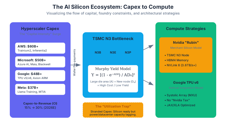
Historically, Hyperscaler Capex was distributed across real estate, networking, and general-purpose CPU servers. However, the emergence of Large Language Models (LLMs) has forced a radical reallocation. We are witnessing a shift in Capital Intensity, defined as the ratio of capital expenditures to total revenue.
What it is
Hyperscaler Capex refers to the billions of dollars invested by cloud service providers to build and equip datacenters. In the AI era, this is increasingly concentrated in Accelerated Compute—GPUs and TPUs—and the specialized high-bandwidth memory (HBM) and networking fabric required to connect them.
Why it matters
The sheer scale of investment acts as a "moat." By front-loading billions in prepayments to foundries like TSMC, Hyperscalers are effectively "cornering the market," leaving smaller players and even sovereign nations to fight for the remaining wafer starts.
The Economics of Capex Intensity
To understand the magnitude, consider the Capex-to-Revenue Ratio ($CI$): $$CI = \frac{\sum \text{CapEx}}{\text{Total Revenue}}$$
In the pre-AI era (2018-2021), Google and Microsoft maintained a $CI$ of approximately 12–15%. In the 2024-2026 forecast, this is projected to surge toward 25–30%.
| Hyperscaler | 2023 Capex (Actual) | 2024/25 Capex (Est.) | Primary Focus |
|---|---|---|---|
| Microsoft | ~$32B \vert ~$50B+ | Azure AI, Nvidia H100/B200, Maia | |
| ~$32B \vert ~$48B+ | TPU v5/v6, Axion ARM CPUs | ||
| Meta | ~$28B \vert ~$37B+ | Llama 3/4 Training, MTIA | |
| AWS | ~$48B \vert ~$60B+ | Trainium2, Inferentia2, Graviton |
Common Pitfalls: The "Utilization Trap"
A common misconception is that higher Capex automatically leads to higher revenue. However, the Time-to-Value (TTV) for AI silicon is lengthening. If a Hyperscaler spends $10B on Nvidia Blackwell clusters today, but the power utility cannot provide the 500MW required to run them for 18 months, the Capex becomes "stranded capital," dragging down Return on Invested Capital (ROIC).
The N3 Node Bottleneck and the "Rubin" Transition
As the industry moves toward the TSMC N3 (3nm) family of process nodes, a structural supply-demand imbalance has emerged. This is not merely a matter of building more factories; it is a fundamental limit of lithography and material science.
What it is: The N3 Family
TSMC’s N3 is the last major node to utilize FinFET (Fin Field-Effect Transistor) architecture before the transition to GAAFET (Gate-All-Around) at N2. However, N3 is not a single node but a complex roadmap:
- N3B: The initial "Base" node (used by Apple).
- N3E: The "Enhanced" node, optimized for high-performance computing (HPC) and better yields.
- N3P: Further performance and density optimizations.
Why it matters: Nvidia Rubin
Nvidia’s roadmap has accelerated from a two-year cadence to a one-year cadence. Following the Blackwell (B100/B200) architecture, which utilizes TSMC’s 4NP node, Nvidia announced the Rubin platform. Rubin is expected to be the first mass-market AI accelerator to leverage the N3 node at extreme scale, alongside HBM4 memory.
Worked Example: Wafer Utilization and Yield
Consider a hypothetical die for a next-generation AI accelerator on N3E.
- Reticle Limit: ~858 $mm^2$
- Die Size: ~700 $mm^2$ (Large-scale AI chips often push the reticle limit)
- Defect Density ($D_0$): 0.1 defects/$cm^2$
Using the Murphy Yield Model: $$Y = \left( \frac{1 - e^{-A D_0}}{A D_0} \right)^2$$ Where $A$ is the die area. For a 700 $mm^2$ chip, even a slight increase in $D_0$ on a new node like N3 can drop yields below 50%, effectively doubling the cost per functional chip. This is why Hyperscalers are pre-paying: they are paying for the wafers, not the working chips, absorbing the yield risk to ensure they are first in line.
| Feature | Blackwell (N4P) | Rubin (N3) |
|---|---|---|
| Transistor Density | ~125M Tr/$mm^2$ | ~220M Tr/$mm^2$ |
| Memory Type | HBM3e | HBM4 |
| Interconnect | NVLink 5 (1.8TB/s) | NVLink 6 (3.6TB/s+) |
| Packaging | CoWoS-L | CoWoS-R / SoIC |
Google TPU and the Vertical Integration Strategy
While Nvidia dominates the merchant silicon market, Google has pioneered the Vertical Integration model with its Tensor Processing Unit (TPU). This allows Google to bypass the "Nvidia Tax" (estimated at 60-80% gross margins) and optimize the silicon specifically for the TensorFlow/JAX software stacks.
How it works: Systolic Array Architecture
Unlike a GPU, which uses thousands of small threads to manage general-purpose tasks, the TPU uses a Systolic Array.
Definition: A systolic array is a network of data processing units (DPUs) where data flows through the system in a rhythmic fashion, similar to how blood pulses through the heart.
In a Matrix Multiply Unit (MXU), data from memory enters the array and is passed from cell to cell without returning to the main register file at every step. This drastically reduces power consumption and increases throughput for the Matrix-Matrix multiplication ($C = A \times B$) that defines deep learning.
The Economics of TPU vs. GPU
Google’s TPU v5p is designed to compete directly with the H100. By controlling the entire stack, Google achieves a significantly lower Total Cost of Ownership (TCO).
| Metric | Nvidia H100 (Merchant) | Google TPU v5p (Internal) |
|---|---|---|
| Acquisition Cost | ~$30,000 - $40,000 | ~$5,000 - $8,000 (Est. COGS) |
| Software Stack | CUDA (Closed, Dominant) | XLA / JAX (Optimized for TPU) |
| Memory Architecture | HBM3 | Custom HBM Implementation |
| Deployment | Universal | Google Cloud Only |
Concrete Example: TCO Derivation
Let $C_{chip}$ be the cost of the chip, $P$ be the power consumption in kW, $R$ be the rack/cooling overhead, and $L$ be the lifespan in hours. $$TCO = C_{chip} + (P \times L \times \text{Cost per kWh}) + \text{Networking Overhead}$$
For a cluster of 10,000 chips:
- Nvidia H100: High $C_{chip}$ ($400M) + High Networking (InfiniBand).
- Google TPU: Low $C_{chip}$ ($80M) + Proprietary Optical Circuit Switching (OCS).
Even if the TPU is 20% less performant than the H100 in raw FLOPS, the TCO advantage makes it the superior choice for internal workloads like Gemini training.
Foundry Diversification: Breaking the TSMC Hegemony
The "Great AI Silicon Shortage" is, at its core, a TSMC Shortage. TSMC currently commands over 90% of the advanced node market (sub-7nm). To mitigate this "single-source risk," Hyperscalers and chip designers are aggressively pursuing Foundry Diversification.
The Challengers: Samsung and Intel
- Samsung Foundry: Samsung was the first to move to GAAFET (3GAP). While they have struggled with yield issues, their "Turnkey" model—where they provide the logic, the HBM, and the advanced packaging (I-Cube/X-Cube) in one house—is highly attractive to companies like Meta and Groq.
- Intel Foundry (IFS): Intel’s 18A node is the industry’s great hope for a Western-based advanced foundry. The key innovation here is PowerVia (backside power delivery), which separates the power signals from the data signals, allowing for higher clock speeds and better thermal management.
Comparative Analysis of Advanced Nodes
| Parameter | TSMC N3E | Samsung 3GAP | Intel 18A |
|---|---|---|---|
| Transistor Type | FinFET | GAAFET (MBCFET) | GAAFET (RibbonFET) |
| Power Delivery | Front-side | Front-side | Backside (PowerVia) |
| Key Customer | Apple, Nvidia, AMD | Groq, Tenstorrent | Microsoft, DoD |
| Risk Profile | High (Geopolitical) | Medium (Yield) | Medium (Execution) |
Why Diversification is Hard: The "Porting" Problem
Moving a design from TSMC N3E to Intel 18A is not a simple "Save As" operation. It requires:
- PDK (Process Design Kit) Alignment: Re-characterizing every standard cell and SRAM bitcell.
- IP Availability: Ensuring that high-speed SerDes (for networking) and HBM controllers are available and validated on the new process.
- Packaging Parity: TSMC’s CoWoS (Chip on Wafer on Substrate) is the industry standard. Samsung and Intel must prove their 2.5D/3D packaging can match TSMC’s thermal and signal integrity.
Memory and Interconnect: The Hidden Bottlenecks
While much focus is on the logic (the GPU/TPU), the actual "winner" of the supply chain wars is often the one who secures the HBM (High Bandwidth Memory) and the Packaging.
HBM3e and the HBM4 Transition
AI accelerators are "memory-bound," meaning the processor spends most of its time waiting for data from memory. HBM addresses this by stacking DRAM dies vertically and connecting them directly to the processor via a wide interface (1024-bit for HBM3e, 2048-bit for HBM4).
The CoWoS Crunch
TSMC’s CoWoS is the "secret sauce." It is a middle-layer silicon interposer that allows the GPU and HBM to communicate at massive speeds. The shortage of CoWoS capacity in 2023-2024 was the primary reason for Nvidia's lead times stretching to 52 weeks.
Key Insight: In the current market, owning the wafer start is useless if you do not have a guaranteed slot in the CoWoS packaging line. This is why "Foundry Diversification" must also include "Packaging Diversification."
Summary of the 'Winners'
In the Great AI Silicon Shortage, the winners are determined by three factors:
- Capital Depth: The ability to write $10B+ checks for prepayments.
- Architectural Flexibility: The ability to design custom silicon (TPUs/ASICs) when merchant silicon (Nvidia) is unavailable.
- Supply Chain Sophistication: Managing the "Golden Triangle" of Logic (TSMC), Memory (SK Hynix/Samsung), and Packaging (CoWoS).
| Category | Winner | Reason |
|---|---|---|
| Merchant Silicon | Nvidia | Software moat (CUDA) and rapid release cadence (Rubin). |
| Vertical Integration | Decade-long head start in TPU development and OCS networking. | |
| Foundry | TSMC | Unrivaled yield and the CoWoS ecosystem. |
| Memory | SK Hynix | First-mover advantage in HBM3e mass production. |
AI_QUIZ. Why is the transition from N3E to N2 significant for AI hardware?
- A) It introduces the first 1024-bit memory interface.
- B) It marks the shift from FinFET to GAAFET architecture.
- C) It eliminates the need for CoWoS packaging.
- D) It is the first node to use 193nm immersion lithography.
-
What is the primary economic advantage of Google's TPU over Nvidia's GPUs for internal Google workloads?
- A) Higher resale value on the secondary market.
- B) Lower Total Cost of Ownership (TCO) by avoiding merchant margins.
- C) Ability to run Windows-based legacy applications.
- D) Lower power consumption due to x86 compatibility.
-
In the context of foundry diversification, what does "PowerVia" refer to?
- A) A new type of high-voltage battery for datacenters.
- B) Intel’s backside power delivery technology.
- C) Samsung’s wireless charging for mobile chips.
- D) TSMC’s method for cooling HBM stacks.
-
Which bottleneck was primarily responsible for the 52-week lead times for Nvidia H100s in 2023?
- A) Shortage of raw silicon wafers.
- B) Lack of cleanroom janitorial staff.
- C) Limited CoWoS packaging capacity.
- D) Insufficient global shipping containers.
Answers: 1-B, 2-B, 3-B, 4-C
AI_STUDY_GUIDEI_STUDY_GUIDE## Key Terms to Master
- Hyperscaler: Large-scale cloud providers (AWS, Azure, GCP, Meta) that operate massive datacenter fleets.
- Capex Intensity: The percentage of revenue reinvested into capital assets; a key metric for tracking AI investment.
- N3 Node: TSMC’s 3nm process family; the current "bleeding edge" for AI silicon.
- GAAFET (Gate-All-Around): A transistor architecture where the gate surrounds the channel on all sides, reducing leakage.
- CoWoS (Chip on Wafer on Substrate): A 2.5D packaging technology essential for connecting HBM to high-performance logic.
- HBM4: The next generation of High Bandwidth Memory, featuring a 2048-bit interface and direct stacking on logic.
- Systolic Array: A specialized hardware architecture used in TPUs to accelerate matrix multiplications efficiently.
- 18A: Intel’s upcoming process node, intended to compete with TSMC’s 2nm-class nodes.
Critical Thinking Questions
- How does the "prepayment" model for wafers affect the competitive landscape for AI startups compared to established Hyperscalers?
- If Samsung successfully yields its 3GAP node with GAAFET before TSMC stabilizes N2, how might the market share of AI accelerators shift?
- Analyze the trade-off between "Merchant Silicon" (Nvidia) and "Custom Silicon" (TPU/Maia). Under what conditions should a company choose one over the other?
- Why is backside power delivery (PowerVia) considered a "holy grail" for high-performance AI chips?
Source Materials
Study The Great AI Silicon Shortage with AI — Free on Lykke
Sign up for free to generate personalized flashcards, quizzes, and study guides from this course. Chat with an AI tutor that knows the material.
Get Started FreeView this course wiki on Lykke · Browse all public course wikis